| Frequency (GHz) |
1.8~2.7 |
| VCC (Min) (V) |
1.6 |
| VCC (Max) (V) |
3 |
| Gain(dB) |
14.5 |
| NF(dB) |
0.7 |
| Icc (mA) |
6.8 |
| Temperature |
-40℃~85℃ |
| P1dB (dBm) |
-3.8 |
| Package (mm) |
DFN 1.1X0.7-6L |
• Operating frequency:1805~2690MHz
• low noise figure
➢0.7dB noise figure at 1805~2200MHz
➢0.9dB noise figure at 2300~2690MHz
• High power gain
➢14.5dB power gain at 1805~2200MHz
➢13.0dB power gain at 2300~2690MHz
• Insertion loss in bypass mode: 3.5dB
• Supply voltage: 1.6V to 3.0V
• Gain mode current: 6.5mA
• Bypass mode current: <1μA
• Requires only one input matching inductor
• Input and output DC decoupled
• DFN 1.1mmX0.7mm-6L
• RoHS Compliant, Pb-free, Halogen Free
• Moisture Sensitivity Level : MSL1
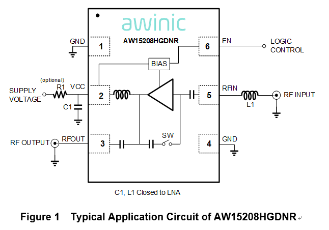
The AW15208HGDNR is a Low Noise Amplifier with bypass mode for LTE middle band and high band receiver applications. The AW15208HGDNR requires only one external input matching inductor, reduces assembly complexity and the PCB area, enabling a cost-effective solution.
The AW15208HGDNR achieves low noise figure, high linearity, high gain, over a wide range of supply voltages from 1.6V up to 3.0V. All these features make AW15208HGDNR an excellent choice for LTE LNA as it improves sensitivity with low noise figure and high gain, provides better immunity against jammer signals with high linearity, reduces filtering requirement of preceding stage and hence reduces the overall cost.
The AW15208HGDNR is available in a small, lead-free, RoHS-Compliant, DFN 1.1 mm x 0.7 mm x 0.37 mm-6L package.